The Modular Read-Out Controller for CBM
CBM ROC
The CBM experiment at FAIR consists of a number of different detectors which require the readout of multiple detector frontend electronics. This is usually done with special FPGA based read-out controller (ROC) boards. The different detectors assemble different frontend electronics requiring different ROCs or at least different ROC firmwares. However, the interface in the other direction of the readout chain - towards the computing nodes - is usually quite the same for all the readout logics of the different detectors. On the other hand, for the direction towards the computing nodes one has to deal with different scenarios.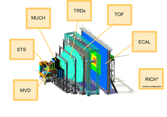
A Modular ROC design
All together, this led to the idea of a modular ROC design, which separates the FPGA firmware into a readout logic module and a transport logic module. The functionality of the transport logic can be re-used for all detectors, only the interface to the frontend electronics needs to be exchanged. Once the transport module for the final detector setup is finished it becomes available for all detectors with minimal effort.
In addition, this modular approach allows an efficient development of the firmwares by more than one designer. The frontend modules and the transport modules can be developed separately by different developers.
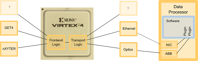
Of course the modules have to share a common interface. The interface is separated in three different classes, a OPB (On-chip Peripheral Bus) like interface for the slow control, a FIFO interface for data transport and a deterministic latency interface for synchronization using so called DLM messages. The interface is designed to respect the special requirements of the self-triggered and time-stamped concept of the CBM experiment.
The modules that are supposed to be used in the final experiment (and only those) need to be designed tolerant against Single Event Effects because of the exposition to ionizing radiation. Fault tolerance for FPGAs means a consideration of multiple logical hardware layers. It has to start with the coverage of static LUT and routing content via the so called "Scrubbing" method, provided exclusively by Xilinx Virtex FPGAs. Static partial bitstream content is continuously written to the chip via the SelectMAP configuration interface whereas present bit-flips are instantly overwritten at runtime. This feature has been realized using an additional controller connected to flash memory which contains the partial configuration files. It is performed automatically and requires no user interaction at runtime. More complicated is the conservation of dynamic chip content like flip-flop and BRAM data, which is regularly underlying major changes during system runtime. These elements have to be considered at the logical design layer. Well known principles like Double and Triple Modular Redundany are used in conjunction to voters and loopback circuits to avoid accumulation of single bit errors and keep important data valid. Finite state machines for example have to avoid illegal transitions between defined states as well as unknown behavior or reset when entering illegal states. This can be realized by introducing state encoding using a hamming distance of at least 3. The encapsulated integration of fault tolerance to modularized FPGA components enables a selective coverage of design content and thus is totally transparent to connected modules, which may not provide such features.